
iQrypto / Technology
How the quantum entropy cell works.
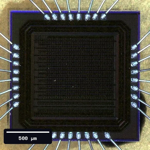
A cell under 5 µm, validated in silicon on a European 180 nm CMOS process.
The physics, in one paragraph
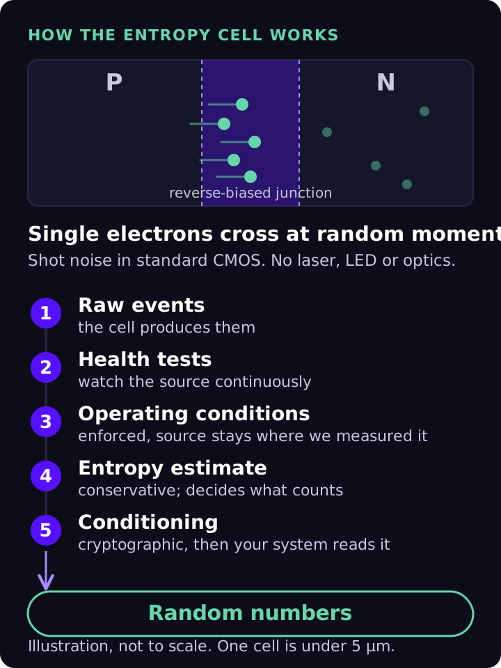
Our entropy source is a reverse-biased, deliberately high-leakage PN junction in standard CMOS. Defect-assisted transitions create single electron and hole pairs at random moments: a discrete, Poisson process whose next event cannot be predicted, even in principle.
We count the electrons, watch the source continuously with health tests, and condition the output into random numbers. There is no laser, no LED and no optics.
Want to see a public randomness demo? Explore QRNG.io (opens in a new tab). It is an independent demonstration, not an iQrypto product.
The numbers
- Cell size
- Under 5 µm
- Cell power
- Under 1 nW on average, cell only
- Today's chip
- 1.5 × 1.5 mm die, under 15 mW in total
- Raw entropy today
- Over 150 bits per second per cell. Cells run in parallel.
- Next-generation performance
- About 10 times faster than the current chip, from our internal measurements.
- Entropy
- 0.99 bits per bit, from our internal NIST SP 800-90B assessment
- Process
- Standard CMOS on a European 180 nm process. No light source and no exotic steps.
Smaller than a red blood cell.
Inside the hardware, the quantum entropy cell is under 5 µm. Compare the source, the 100 × 100 µm integration block and the 1.5 × 1.5 mm chip die below.
The axis is logarithmic: 10 µm, 100 µm and 1 mm are equal tenfold steps. The red blood cell is a typical-size reference.
Add cells, add speed.
One cell is tiny, and cells work in parallel. The IoT-class integration block measures 100 × 100 µm. A full die serves high-throughput systems. You size the block to the product.
Why integration matters.
When the entropy source sits inside the chip that uses it, random numbers never travel over an external bus that can be probed. There is no extra part on the board, no extra package and no extra power rail.
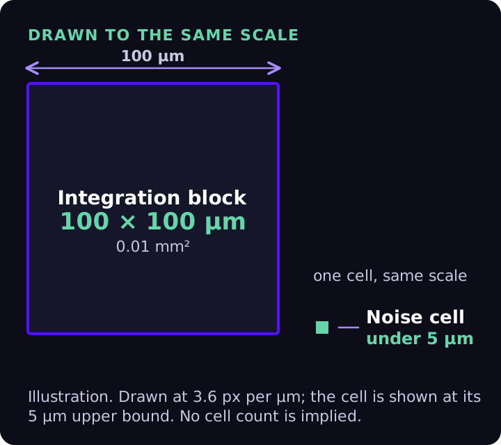
100 × 100 µm, scaled to billions of devices.
Each integration block occupies 0.01 mm². In an illustrative scenario with 8.2 billion blocks, their combined footprint would be about 82 m² of silicon.
Block-area calculation: 0.1 mm × 0.1 mm × 8.2 billion = 82 m². Wafer margins, manufacturing yield losses and packaging add to the resources required.
Evidence and assurance
Our design follows the same chain that standards ask for. Each step is something you can test.
Formal NIST SP 800-90B validation and AIS 31 readiness are on our roadmap. Today's figures come from our own internal assessment.
- A characterised physical source
- Enforced operating conditions
- A conservative entropy estimate
- Continuous health tests
- Cryptographic conditioning
Intellectual property
Our random-number-generator technology is protected by granted patents. Patent family WO 2021/240143, "Random number generator".